CCD Chips: Silicons That Turned Photons into Perfect Digital Eyes
CCD chips convert photons into electrons via the photoelectric effect in silicon, powering digital cameras, space telescopes, and X-ray detectors with near-perfect quantum efficiency and ultra-low noise.
Remember the days when telescopes still relied on fragile photographic plates? Those glass sheets coated with light-sensitive chemicals captured starlight the slow, imperfect way. Today everything changed thanks to a quiet silicon hero: the charge-coupled device, or CCD.
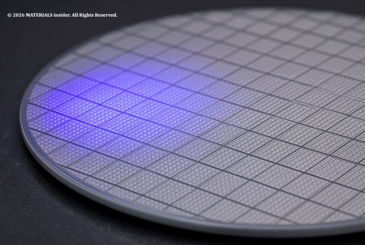
CCDs sit at the heart of digital cameras, space telescopes, medical imagers, and scientific instruments. They turn incoming photons into clean electrical signals that a computer can read instantly. The principle is pure physics, yet the engineering is pure materials science.
It all starts with the photoelectric effect, the same phenomenon Albert Einstein explained in 1905. When a photon with enough energy hits an atom in the outer shell of silicon, it can knock an electron free. Silicon is ideal because visible light easily liberates these electrons.
A thin silicon wafer acts as the stage. Each tiny positively charged capacitor sits above a small region of the wafer and collects the freed electrons. One photon ideally frees one electron — that is 100 % quantum efficiency. The best modern CCDs reach about 90 %. For comparison, the rods and cones in the human eye manage only around 1 %.
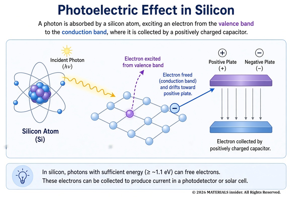
As soon as the shutter opens, photons begin producing electrons. The capacitors keep collecting until the shutter closes. The voltage across each capacitor then tells the computer exactly how many electrons arrived. That voltage becomes one pixel. Thousands or millions of these pixels form a complete image array.
Hubble’s Wide Field Camera 2 used two 2K-by-4K arrays for an 8-megapixel CCD. Color came from separate exposures through filters — blue for oxygen, green for hydrogen, red for nitrogen — then combined into the famous planetary nebula images we still admire.
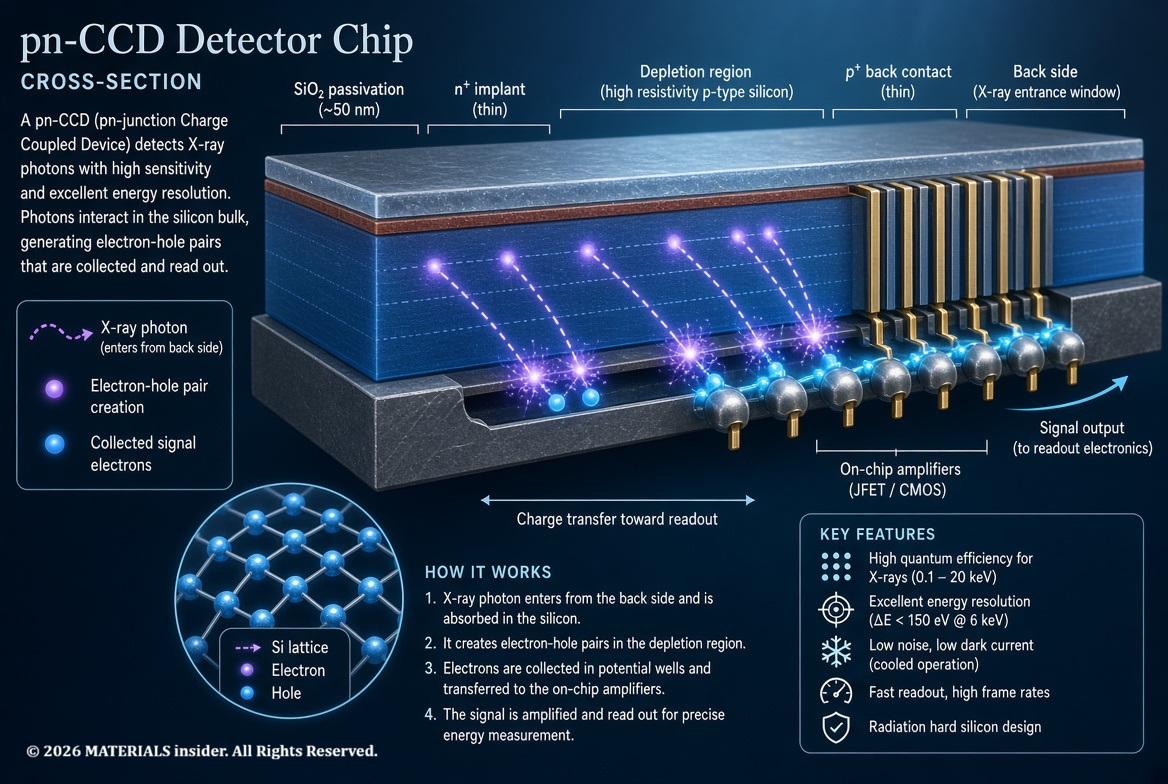
Special versions go further. The pn-CCD developed for ESA’s XMM-Newton X-ray mission integrates the first amplifier right on the same silicon chip. Researchers reduced total input capacitance, improved transistor transconductance, and refined the p-well implant. The result? Equivalent noise charge dropped to just 2.2 electrons at the operating temperature of 150 K — and only 8.8 electrons even at room temperature. That ultra-low noise lets astronomers measure faint X-ray photons with energy resolution better than 60 eV at 1 keV.
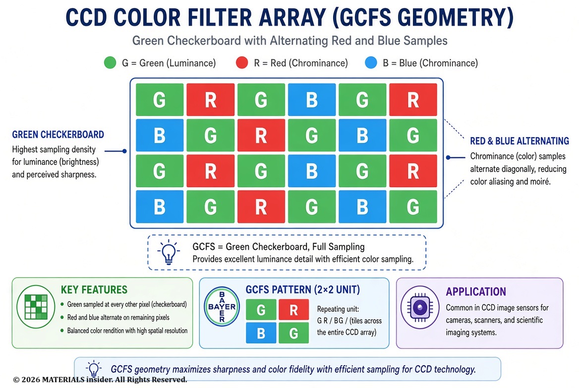
For everyday color cameras the challenge is different. A single-chip CCD must separate red, green, and blue from one continuous stream of data. Engineers designed clever color-filter arrays such as the green-checker field-sequence (GCFS) geometry. This pattern keeps green samples on a checkerboard while alternating red and blue between fields, eliminating horizontal color errors that plagued earlier Bayer layouts.
A dedicated color-signal-separation IC then uses CCD delay lines, sample-and-hold circuits, and dual-clamp stages to reconstruct clean RGB channels. Vertical peaking corrects abrupt brightness changes, restoring resolution without introducing false colors. The final system delivered 340 TV lines of horizontal resolution with no visible color artifacts.
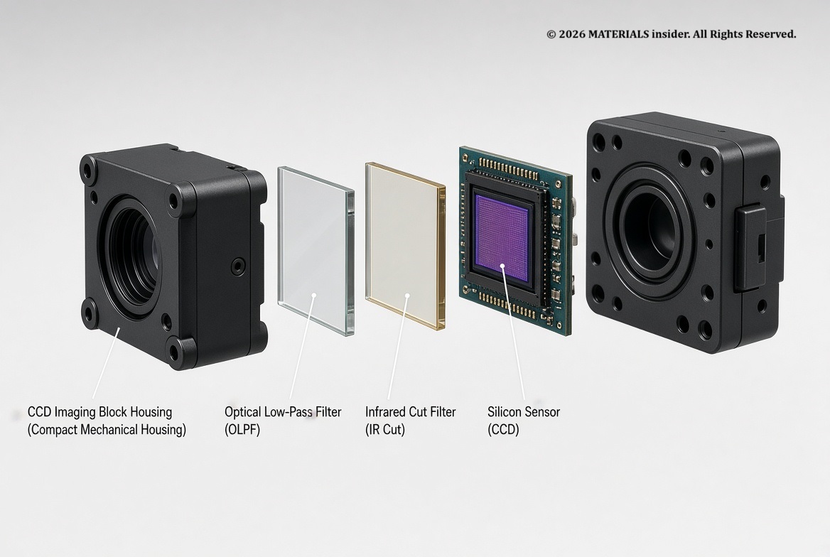
To make these sensors practical in compact cameras, the entire optical path was engineered into a single CCD Imaging Block. Optical low-pass filters (Savart plates) suppress aliasing, an infrared cut filter balances the spectral response, and precise mechanical mounting guarantees focus and alignment without adjustment. The finished block weighs only 26 g and delivers 330 TV lines of resolution — a complete imaging system that simply screws onto a lens.
All of this rests on silicon’s unique materials properties: its bandgap matches visible light, its crystal lattice allows precise doping and implants, and its native oxide supports the delicate gate structures that create the potential wells holding each charge packet.
From Einstein’s 1905 insight to Hubble’s deep-space portraits and the smartphone in your pocket, CCD chips show what happens when materials science meets quantum physics. They remain one of the most elegant bridges between the photon and the digital bit.
References
Pinotti et al., “The pn-CCD on-chip electronics,” Nucl. Instrum. Methods Phys. Res. A 326 (1993).
Watanabe et al., “A CCD Color Signal Separation IC for Single-Chip Color Imagers,” IEEE J. Solid-State Circuits 19 (1984).
Ogawa et al., “Development of CCD Imaging Block for Single Chip Color Camera,” IEEE Trans. Consum. Electron. 31 (1985).
Boyle & Smith, original CCD papers, Bell Syst. Tech. J. (1970).
ESA XMM-Newton pn-CCD performance reports.

Space Shuttle Challenger Disaster (1986)
The Space Shuttle Challenger disaster was NOT caused by a rocket engine failure or software malfunction. The root cause was the loss of sealing performance in rubber O-rings located within the Solid Rocket Booster.
Read Full Article →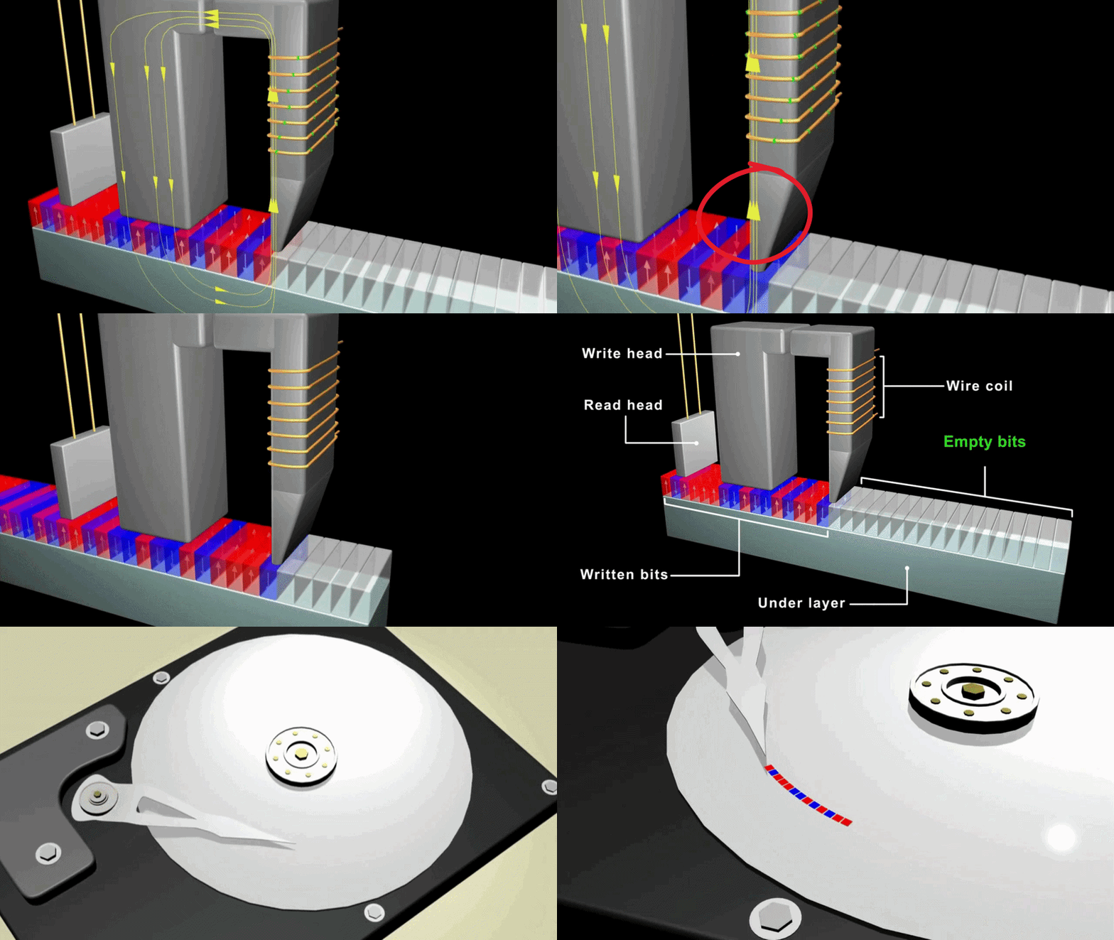
Magnetism for Recording Devices
Magnetism in ferromagnetic materials is the hidden physics that lets hard disks & magnetic tapes store digital data for without power. Data storage is not an electronic process but a property of the materials.
Read Full Article →Share this article:
Advertisement 1/4
Advertisement 2/4
Advertisement 3/4
Advertisement 4/4